Why should FPGA avoid combinational logic loops?
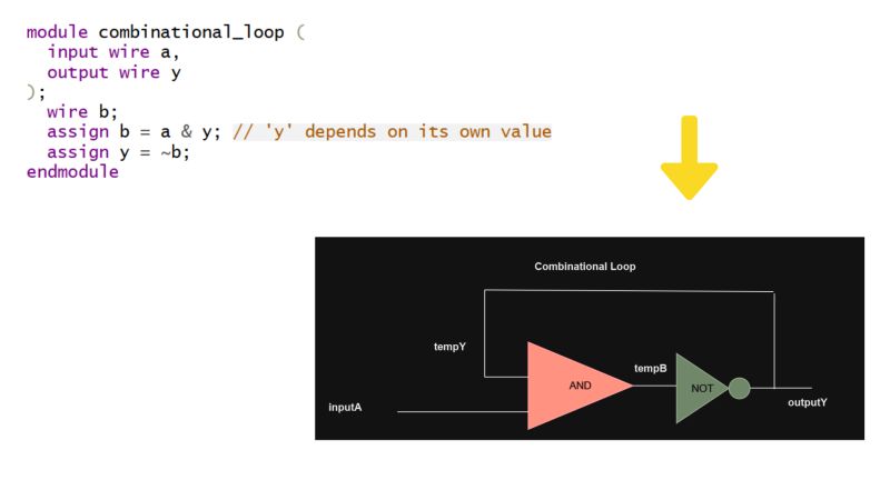
In short, combinational loops should be avoided in FPGAs (and all synchronous digital design) because they create unpredictable, unstable, and race-condition-prone circuits that violate the fundamental principles of synchronous design.
Here’s a detailed breakdown of why they are so problematic:
1. They Create Unstable States and Oscillations
A combinational loop has no inherent memory. The output can continuously change based on its own previous output, creating a race condition that often results in high-frequency oscillations or settles into a metastable state.
Example: Imagine a simple loop where the output of a NOR gate is fed directly back to its input (e.g., if one input is held at '0').
The gate has a propagation delay.
The output will oscillate with a period roughly twice that delay. This is not a useful clock; it's a chaotic signal that consumes power and creates noise.
2. They Violate the Principles of Synchronous Design
Modern FPGA design is built on the synchronous paradigm, which uses clock signals to control the timing of all operations. Combinational loops break this model.
No Defined Timing Path: Static Timing Analysis (STA) is the tool used to guarantee an FPGA design will work at a specified clock speed. STA works by analyzing paths that start at a register (flip-flop) and end at a register.
Analysis Impossible: A combinational loop has no starting or ending register. The tools cannot determine its delay or whether it can meet timing constraints. This makes the design's behavior unverifiable and unreliable.
3. They Cause Timing and Race Conditions
Even if a loop seems to work in simulation (which often has idealized, zero-delay models), it will behave differently in real hardware due to gate and routing delays.
Glitches and Hazards: The signal can oscillate or produce short glitches before (theoretically) settling to a stable value. These glitches can be incorrectly captured by downstream registers, leading to functional errors.
Dependence on Physical Layout: The behavior of the loop can change based on how the FPGA place-and-route tool happens to layout the design. A minor change in the code or constraints could cause the loop to behave completely differently, making the design non-deterministic and non-portable.
4. They Lead to Power and Noise Issues
A rapidly oscillating loop:
Consumes Dynamic Power: The constant switching of logic gates draws significant current.
Generates Noise: The high-frequency oscillations can create electrical noise on the power supply, potentially affecting other, stable parts of the design and causing unexpected failures.
How Do Combinational Loops Happen?
They are often created accidentally by designers, usually due to poor coding practices. Common scenarios include:
Incomplete conditional statements:
verilog
 // BAD CODE: Creates a latch AND a potential loop if 'sel' is not always 1.
 always @(*) begin
     if (sel)
         out = a;
     // else out retains its previous value -> implied latch -> feedback loop
 end
The implied latch creates a memory element, but it's built from combinational feedback in the FPGA's lookup tables (LUTs), not a dedicated flip-flop. This is unstable.
Asynchronous feedback in "combinational" logic:
verilog
 // BAD CODE: Direct asynchronous feedback.
 assign out = (sel & a) | out; // If sel is 0, out = out. This is a loop!
Mistakes in state machine design where output logic accidentally feeds back into itself without a register.
How to Avoid and Fix Them
Use Strict Coding Guidelines:
For combinational
alwaysblocks, usealways @(*)oralways_comb(SystemVerilog) and assign every output for every possible branch of aniforcasestatement. Use adefaultassignment at the top of the block.Never allow a variable to hold its value implicitly.
verilog
    // GOOD CODE: No implied latch, no loop.
    always_comb begin
        out = 1'b0; // Default assignment
        if (sel) begin
            out = a;
        end
    end
Use Synchronous Design Patterns:
Always use registers (flip-flops) to hold state. All feedback paths must be clocked.
The only loops in your design should be the intentional ones that go from register outputs -> through combinational logic -> back to register inputs. This is the foundation of state machines and pipelined logic.
Rely on Tools:
- Modern synthesis tools (like those from Xilinx/Vivado and Intel/Quartus) are very good at warning you about inferred latches and combinational loops. Never ignore these warnings! Treat them as errors.
Summary Table
| Aspect | Without Combinational Loops (Good Design) | With Combinational Loops (Bad Design) |
| Stability | Stable, predictable behavior | Unstable, oscillates or is metastable |
| Timing | Can be analyzed and verified with STA | Impossible to analyze; unpredictable |
| Reliability | Deterministic and portable | Behavior changes with layout and temperature |
| Power | Predictable power consumption | Excessive power draw from oscillations |
| Design Flow | Supported by all tools and methodologies | Violates fundamental design rules |
Conclusion: Combinational loops are forbidden because they create analog-like behavior in a digital system, breaking the deterministic, verifiable model that synchronous FPGA design relies upon. Always use registered feedback to create controlled, stable state.


